Electronic Design Services
We're providing custom electronic design services software and hardware


We provide In-House all electronic design services needed for custom product development. Both software and hardware, DSP, MCU, FPGA, custom PCB design services and mechanical enclosure. We can perform a full turnkey project, or any portion of it according to customer's preference.

Bluetooth, Lora, GSM, 2.4Ghz, 868 / 915Mhz, Wifi, Positioning systems using UWB, custom FMCU Radars, mmWave Radars

Various CMOS Cameras, RT video systems, custom compression algorithms, modification of JPEG, motion estimation in DCT domain, sensor control algorithms, LCD interfaces and GUI device drivers

Various TCP/IP stack modifications, AES-CBC sw and hw, VLAN 802.1q, MAC drivers, SGMII integration, PHY control, USB custom drivers

Various drivers for SD, eMMC, CF, NOR and NAND flashes. Custom high speed FAT32, NAND wear leveling and bad block management, encryption, custom booting modes and second stage loaders

Multiplexed ADC interfaces, hw and sw filters, ultra low THD+N audio systems, condenser studio microphones, phased array audio output, ultrasound rx / tx systems, mp3, various algorithms


We have over 15 years of experience with electronic engineering and we offer in-house schematics & layout services. We also source the PCB and components and handle all operations until assembled boards are at hand

According to the requirements we can: minimize BOM cost / power consumption / board size, improved noise immunity / heat transfer, increase battery life etc...

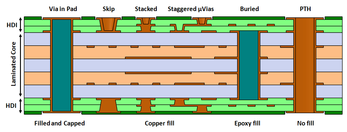
In addition to regular multi-layers, we can offer HDI boards / uVias / blind / buried vias / bendable Flex boards / Rigid-Flex boards. In case of need, we have tight communication with PCB / assembly factories

We develop any mixture of the above. While no two boards are similar, there are always 'building blocks' which are general purpose and can be reused - reducing risks and speeding up the development

We provide assistance with board bring-up once assembled boards arrive, and we are open to provide debugging support even months afterwards

If required, we can also offer software board support package / drivers and examples. We also offer full turnkey solutions
We could probably write several dozens more of do's and dont's. But if we are to pick only 10 - these would be the ones that are more 'clear cut'. Please note that there are many other issues in which case by case judgment has to be made, weighing the upsides and downsides of the different options


Return currents must be allowed to easily flow back to the source. A proper return path of least impedance is required

Ground and power planes can provide high frequency decoupling for BGA ICs. Try to minimize this 'via damage'

The return current always finds a way back to the source, but doing so can cause EMI, noise or even malfunction

Not only EMI can be worse by ~10db, propagation delay on outer and inner layers can differ by 20%, causing skew

When a high speed signal must switch layers using vias, make sure its return current also has a flow path close by


Usually, vias should be tented with soldermask (at least). This protects the via and avoids solder leaking into the barrel

Certain analog ICs are very sensitive to stray capacitance, carefully cutting the ground plane underneath can really help

Double check your CAD's outputs with an external gerber viewer - for correctness, completeness, and clarity

Fragile ICs on a board may crack and fail when the board is broken from the panel. There are proper ways to do it

With today's PCBs, hardly any room is left to properly annotate everything. Use the assembly drawings for that
We have recently added an in depth guide to PCB vias. It also explains about HDI stackup and reliability issues of through hole vias. We recommend understanding the basics of PCB design even if you just plan to outsource your board.

We are trusted by some of the biggest names in the industry!
Most of our customers have engineers in house, yet they choose to outsource to us:
- Tough projects where the cost of the electronic design services need to be determined upfront.
- For the expertise we have in specific processor or circuit.
- When high degree of optimization is needed, i.e small PCB size, low latency communication, long battery life etc.
- Risky projects where its hard to estimate cost / time.
- Returning customers need no specific reason.


Based in Haifa, Israel, ePiccolo Engineering was established in 2008 by Guy Shemesh. Guy holds a B.Sc degree in electrical engineering from the Technion (Summa Cum Laude) which he graduated in 2002 and now pursuing Masters degree in special education with interest areas in Autism, Tic disorder and Neurobiology in general. Guy served in the IDF in one of the elite technological units of the intelligent forces - working hands-on on DSPs, as well as on electronics and other programmable devices.
Being an engineer in the heart and soul, Guy always ran away from management positions and never hesitated to learn and apply new technologies. He is actively involved in every engineering project to this very day and happily shares knowledge and collaborates with other engineers.
We welcome your inquiry and will try to assist you as much as we can.
We value your inquiry and we will get back to you within one business day.